Our Terms & Conditions | Our Privacy Policy
Business News | India’s Semiconductor Vision Gathers Momentum with 3nm Chip Design and Talent Development Initiatives
New Delhi [India], July 25 (ANI): India is home to nearly 20 per cent of the world’s chip design engineers and building on this strong talent base, the government is facilitating the development of a complete semiconductor ecosystem in India, Union Minister of State for Electronics and Information Technology, Jitin Prasada, informed Lok Sabha on Friday.
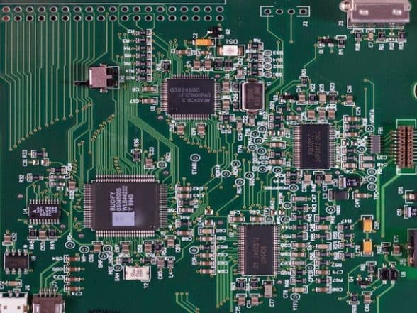
Leading semiconductor companies have established chip design and research centers in India. A 3nm semiconductor chip designed in India was recently unveiled, the minister said.
Also Read | India Open To Share AI Models With Global South, Country’s Linguistic Diversity Can Help in Natural Language Processing Development: IT Secretary S Krishnan.
It showcases the technical capabilities of Indian engineers and importance of Indian design centres in global semiconductor industry.
To foster talent development in the semiconductor chip design, the Government has launched several initiatives, such as, new curriculum by All India Council for Technical Education (AICTE) for VLSI Design and Technology, Integrated Circuit (IC) manufacturing; developing 85,000 skilled manpower in semiconductor design sector & providing EDA tools to design semiconductor chips; 45,000+ students from 100 institutions enrolled so far;
Also Read | LG Q2 Results 2025: LG Electronics Sees 3.1% Decline in Net Profit in 2nd Quarter Amid Rising Logistics and Tariffs Costs.
Besides, a Skilled Manpower Advanced Research and Training (SMART) Lab at NIELIT Calicut is being undertaken to train 1 lakh engineers nation-wide with 44,000+ engineers already trained; collaboration with industry and universities such as Lam Research, IBM and Purdue University.
India is leveraging its large talent pool, global semiconductor design companies are now rapidly expanding their workforce in India to design cutting-edge chips.
Under Semicon India programme, a total outlay of Rs 76,000 crore was approved for catalysing semiconductor and display manufacturing ecosystem in India.
Six (6) semiconductor manufacturing and 22 design-linked incentive (DLI) projects have been approved
72 companies are provided chip design infrastructure such as EDA tools & FPGA (Field Programmable Gate Array) boards from Synopsys, Cadence, Siemens, etc.
Access to the Post Silicon Validation and Testing and Packaging Support is also being provided, the minister noted. (ANI)
(The above story is verified and authored by ANI staff, ANI is South Asia’s leading multimedia news agency with over 100 bureaus in India, South Asia and across the globe. ANI brings the latest news on Politics and Current Affairs in India & around the World, Sports, Health, Fitness, Entertainment, & News. The views appearing in the above post do not reflect the opinions of Pune Media)
Images are for reference only.Images and contents gathered automatic from google or 3rd party sources.All rights on the images and contents are with their legal original owners.
Aggregated From –
Comments are closed.