Our Terms & Conditions | Our Privacy Policy
Mixed signal ASICs (Application Specific Integrated Circuits) chip maker EnSilica has established a new engineering hub at The Bradfield Centre on Cambridge Science Park.
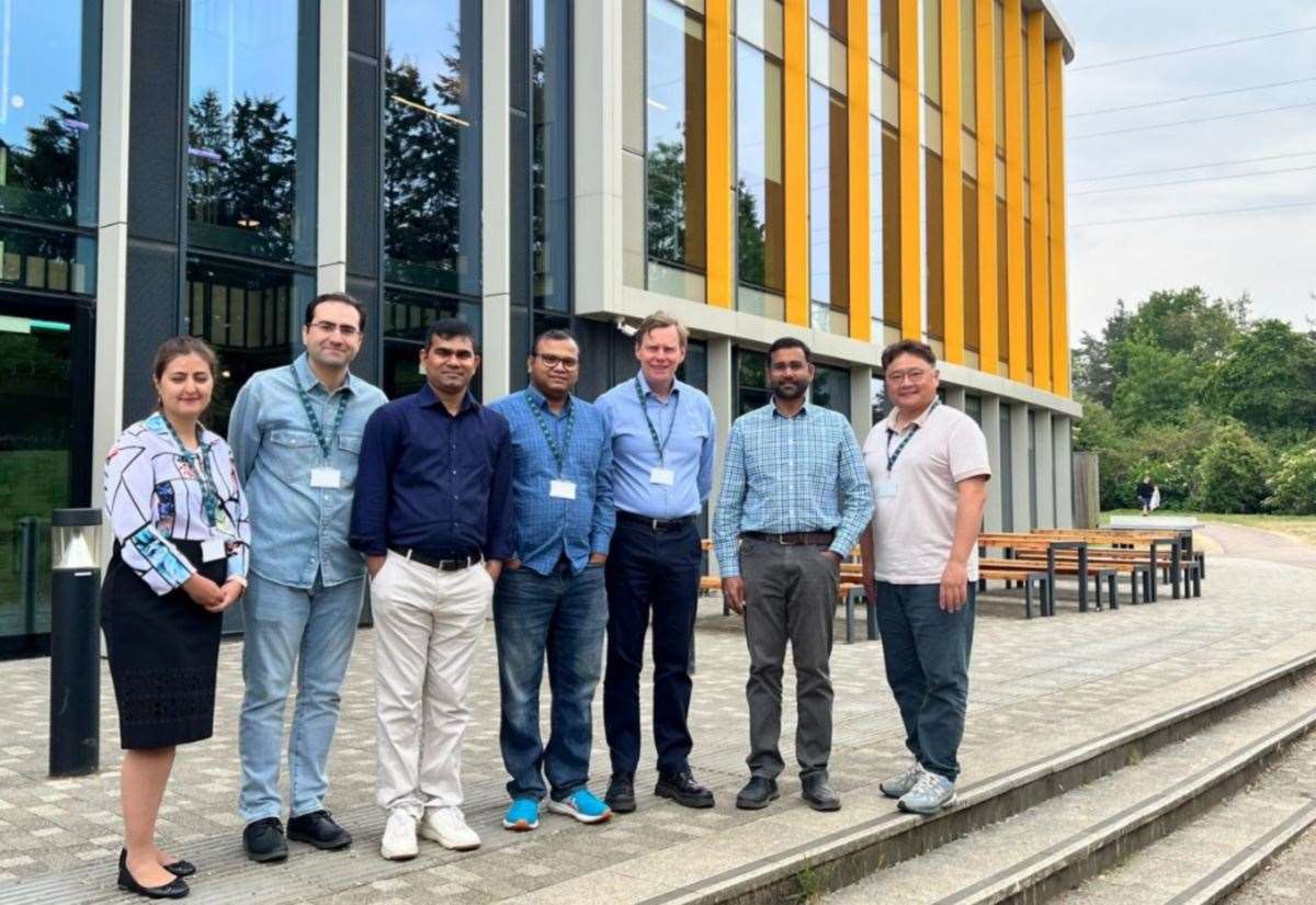
 The EnSilica team at The Bradifled Centre on Cambridge Science Park Picture: Ensilica
Ensilica was founded as a consultancy in 2001, and transitioned to a fabless design and supply business model, in 2016, leveraging its extensive industry experience. It has since emerged as a leading analog IP company. The fabless design house focuses on custom ASIC ( (Application-Specific Integrated Circuit) design and supply services, to both fabricate and test their latest analog IP products.
The integration of analog IP onto a complex silicon chip is a time-consuming process that is exacerbated by the variable quality of currently available analog IP products. Ensilica speeds up the process of proving and qualifying analog IP, and reduces the time-to-market and risk of IC development cycles through a revolutionary top-down delivery of initial IP views.
With the addition of this new facility and technical expertise, EnSilica will expand its existing mmWave/RF integrated circuit design capabilities, an area in which the company has already seen significant customer demand. The expansion has been facilitated by the recent UK Space Agency C-LEO funded award, alongside additional contract momentum and customer wins that continue to support the company’s growth.

 The Bradfield Centre. Picture: Keith Heppell
The city’s new engineering facility has already recruited six engineers, four of whom hold PhDs, which brings the company’s global workforce to 190.
EnSilica currently operates across three UK engineering design centres in Abingdon, Sheffield and Bristol, alongside additional international engineering facilities in Bangalore, India, and Porto Alegre and Campinas in Brazil.
Ian Lankshear, CEO of EnSilica, said: “We are delighted to have not only secured a team of highly skilled engineers at a time when there is a very real shortage of engineering talent in the UK, but also to establish a firm base in an established UK tech hub like Cambridge which ideally positions the business to attract additional talent.
“By further expanding our engineering knowhow across the satellite and communications market, I believe that this investment will enable the business to capitalise further on very real and near-term growth opportunities.”
Images are for reference only.Images and contents gathered automatic from google or 3rd party sources.All rights on the images and contents are with their legal original owners.
Aggregated From –
Comments are closed.