Our Terms & Conditions | Our Privacy Policy
‘Nano Dimension sees Additively Manufacturing Electronics as part of its core.’ – Nano VP of AM Nir Sade
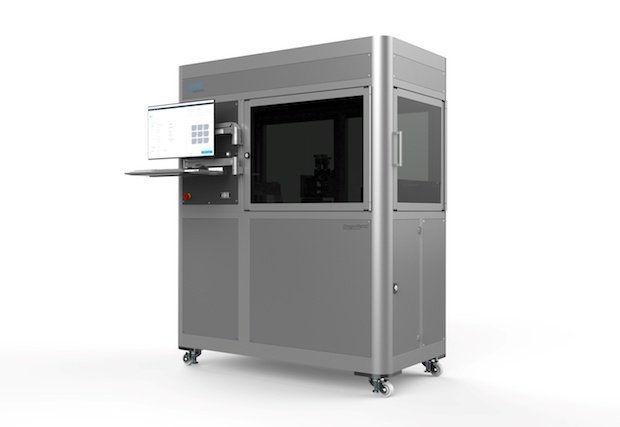
In 2014, Nano Dimension emerged with its Additive Manufacturing Electronics (AME) technology – a process that carries similarities to PolyJet 3D printing technology in the way it lays down material to produce components like printed circuit boards.
Back then, the company was somewhat of an industry minnow, operating within a niche of a niche. In more recent years, you’d be forgiven for forgetting that Nano even still dabbled in the area of AME, given its focus on inorganic growth via a series of high-profile acquisitions, such as the recent deals involving Desktop Metal and Markforged.
As it entered 2025 with a new leadership, it became apparent that there would be much change at Nano this year. Already the company is exploring the strategic alternatives for Desktop Metal, and the Admatec, DeepCube, Fabrica, and Formatec businesses have all been shut down.
One business activity that looks set to remain is the AME offering. So, TCT recently caught up with Nir Sade [NS], Nano Dimension’s Senior Vice President of Additive Manufacturing, to discuss the current status of AME and the opportunities moving forward.
TCT: Nir, Nano Dimension came to market with its Additive Manufacturing Electronics technology around a decade ago. Remind us how the technology works.
NS: We are using two inks – one a conductive ink, silver nanoparticle, and the second is the dielectric ink, which is a polymer-based acrylate that is UV curable – printing both simultaneously, layer over layer, and using a digital file similar to the 3D printing of mechanical parts. And then at the end, we have a functional electronic device which is ready for the assembly part along the line.
Similar to additive manufacturing, it enables freedom of design, on-site production, in-house proof of concepts, reducing dramatically the time to market.
TCT: You mentioned the materials that you are able to process today. Can you share more about the capabilities of those materials?
NS: First, our focus in the last few years has been on the development of materials because we are aiming for functional devices and as we are aiming towards providing an industrial grade solution, we fully understand that materials are key, and that we need to develop materials that would perform very similarly to materials in the traditional manufacturing, and in some cases better.
Now, the materials that we have in our offering today are two materials. One is this silver nanoparticle conductive ink, suspended in a solvent ink, printed using inkjet and then dried and sintered using IR energy, enabling us to get to a conductivity level of about 35%. This is not full aligned with current industry [standards] but for a wide variety of applications, this property is good enough, and on our roadmap, we are developing changes to the material and to the printing process in order to get to higher conductivities, to a certain level that would cover about 90% of the applications out there.
The dielectric material, meanwhile, provides the mechanical part of the design, as well as the dielectric properties. In the last few years, we were focused mainly on the development of a new dielectric material that will enable mechanical and thermal properties that are, I would say, similar to the industry standard. The industry standard is an FR-4 material, a flame retardant material, and this material is undergoing some processes, such as solder reflow for the component assembly at 240 to 260 degrees. Our current material enables solder reflow up to 170 to 190 degrees and we are now at a customer testing of the new material that will be available very shortly.
TCT: You’ve mentioned that the adoption cycle of AME involves an education phase – so what does the company proffer as the key advantages of AME vs conventional methods of manufacture?
NS: I would start with a real market example. The discussions we have had with defence customers, they are looking to develop a new electronic device, specifically an antenna for airborne devices, and they have decided, with this development of this new device, to start from scratch with AME. Why? Because they understood that it will enable them to get better benefits in regards to having a lightweight device neutralisation, but also better performance with a shorter time to market.
Manufacturing with traditional, each iteration takes months. Using AME they can print the first iteration, make several designs with some minor changes, and then test them all at once, reducing development time dramatically. Second, using 3D, they can get better performance. And third, they learn that the gap between simulation to the end result is lower.
They have tested the business case of this antenna, and they realised, as this is low volume, producing it with AME would be more cost efficient than using a traditional manufacturing.
TCT: How is the company working to improve its AME offering moving forward?
NS: First, we will go back again to materials. We see materials and printing processes as critical in going to more industrial solutions and offering wider application opportunities, so we will continue to invest more and more on materials. But further on, as we are aiming towards more industrial application – moving from low TRL, prototyping solutions to low volume production, [we need] a full end-to-end solution, higher productivity, closed loop process control, and higher yield. And, obviously, software tools that will enable users to go from design to manufacturing.
TCT: In recent years, Nano Dimension has been involved in several mergers and acquisitions – how important does AME remain for the business?
NS: Obviously, I cannot elaborate on the acquisitions and so on, but I can say, and I will say, that Nano dimension sees AME as part of its core. Nano Dimension was built on AME. This was the starting point, and it is going to continue and stay a core part of the Nano Dimension strategy.
TCT: Finally, what is the market opportunity for AME?
NS: Based on some market research that we were doing, this is a few billions dollar market for the end of this decade. Obviously, this is dependent, in a way, on the adoption of the market and on our offering, but I do believe that with our latest advancements, mainly in materials, this is opening new applications. We see higher interest from customers when they are exposed to these new properties. As we see it, the significant growth has not materialised yet, mainly because of materials. This is clear, and this is the reason why we have spent so much and invested so much on materials in the last few years.
Images are for reference only.Images and contents gathered automatic from google or 3rd party sources.All rights on the images and contents are with their legal original owners.
Aggregated From –
Comments are closed.