Original Coverage & Source Attribution: tspasemiconductor.substack.com
How Kao’s interfacial science, Fujifilm’s photographic chemistry and Ajinomoto’s materials expertise connect established industries to the next generation of chips.
Japan’s semiconductor story extends into places that consumers would rarely associate with chips: detergent laboratories, photographic-film factories and food-chemistry research centers. Companies known for familiar household products have accumulated knowledge about molecules, particles, coatings and surfaces. Those capabilities can become valuable when semiconductor manufacturers encounter increasingly demanding materials problems.
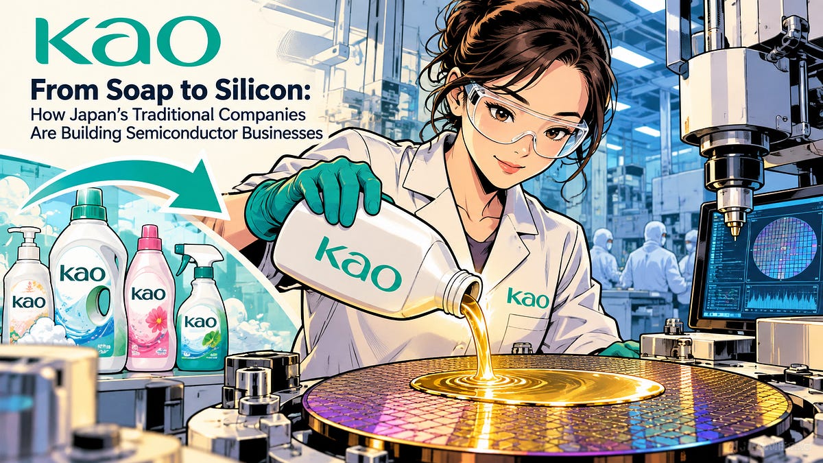
Kao provides a revealing example. Its September 17, 2026 research and development presentation places semiconductor chemicals alongside dermacosmetics as two priority areas for concentrated research investment. The connection is precision control of interfaces: the boundaries where liquids, solids and other materials interact.
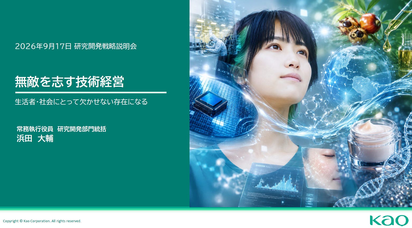
This strategy builds on a substantial industrial history. In the accompanying official Q&A, Kao says its semiconductor-related business has existed for more than 40 years. Its greater visibility in 2026 reflects growing attention and an effort to explain its capabilities. The transformation now underway concerns the scale, technological ambition and strategic importance of that business. Kao’s R&D strategy Q&A.
Kao, Fujifilm and Ajinomoto illustrate how a traditional company can develop a semiconductor growth engine by identifying where its accumulated science solves a difficult manufacturing problem.

Fujifilm Holdings Corporation is a Japanese multinational founded in 1934 as a photographic film maker. After film demand collapsed, it reinvented itself through materials science, using expertise in silver halide and fine chemicals to enter healthcare, electronics, and imaging. Today it supplies medical systems, endoscopes, regenerative-medicine products, semiconductor materials, and high-performance films, while still selling Instax instant cameras and professional imaging gear. Headquartered in Tokyo, Fujifilm operates globally and is often cited as a successful case of corporate transformation from a declining core business into diversified, technology-driven growth.
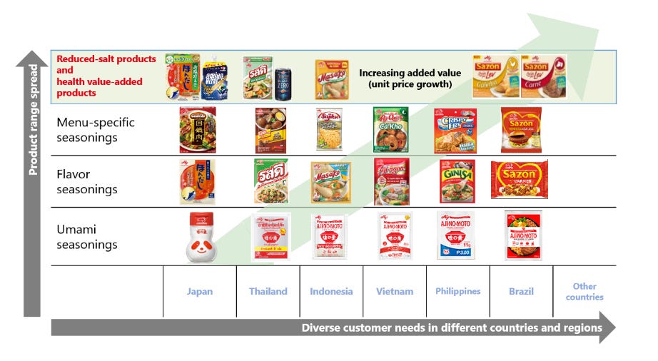
Ajinomoto Co., Inc. is a Japanese food and biotechnology company established in 1909 after scientist Kikunae Ikeda isolated monosodium glutamate, the basis of its famous seasoning. It remains a leading producer of umami seasonings, frozen foods, and amino acids, and has expanded into pharmaceuticals, animal nutrition, and specialty chemicals made by fermentation. The group emphasizes amino-acid science, sustainability, and reducing environmental impact across its supply chain. Based in Tokyo, Ajinomoto sells products in more than 130 countries and is one of the world’s largest producers of amino acids.
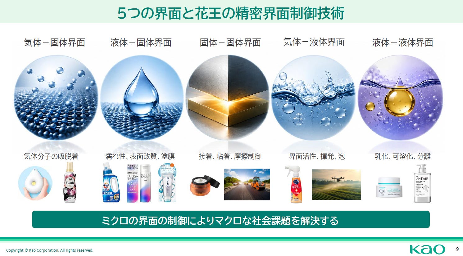
A consumer-product label reveals relatively little about the technical capabilities behind it. Detergents depend on controlling how liquids wet surfaces, how contaminants detach and how removed material remains dispersed. Cosmetics require stable mixtures, controlled film formation and precise interactions between ingredients and surfaces. These problems involve disciplines that also matter in industrial processing.
Kao’s presentation describes five types of interfaces: gas–solid, liquid–solid, solid–solid, gas–liquid and liquid–liquid. Across them, the company studies adsorption, wetting, adhesion, friction, foaming, emulsification and separation. Its historical technology map also includes toner binders, hard-disk polishing agents and other industrial materials, showing how its research has already crossed product categories.
The semiconductor opportunity emerges when this knowledge is translated into a different specification. A formulation must interact with particular materials under particular processing conditions. Its commercial value depends on solving that problem consistently and integrating into the customer’s manufacturing sequence.
From Toilets to Chips: How TOTO Became a Hidden Semiconductor Materials Champion